Product Introduction
High Purity Silicon Target Material: Core Material for Thin Film Deposition
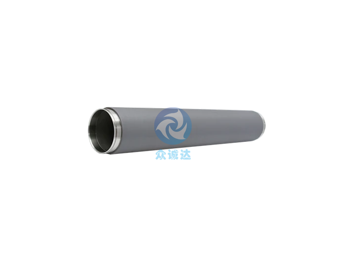
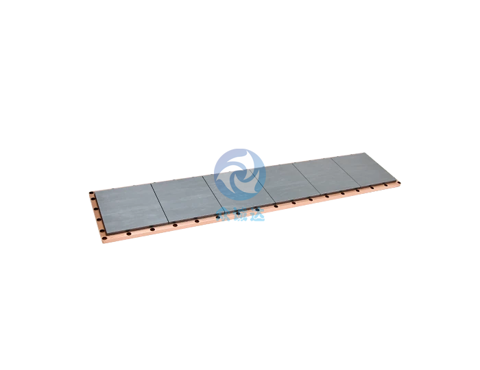
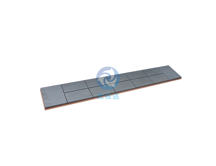
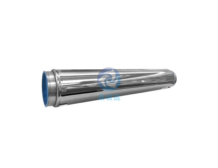
Silicon target material is used in physical vapor deposition (PVD) processes, primarily for depositing medium layers such as silicon oxide, silicon nitride, and silicon hydride. It can be divided into crystalline silicon and HSi types. Silicon targets are typically dark gray with a semi-metallic appearance and a density of about 2.33 g/cm3. The melting point of silicon is 1414°C, and its boiling point is 3265°C. Silicon has a high thermal conductivity coefficient (149 W·m?1·K?1) and excellent thermal conductivity. Additionally, silicon target material has good hardness, optical properties, wear resistance, and excellent corrosion resistance.
Excellent Properties of Silicon Target Material:
High Purity Ensures Stable Thin Film Performance
Crystalline silicon has a purity of 99.999%, while HSi purity is 99.99%
Excellent Thin Film Uniformity and Density
Silicon targets have a high sputtering efficiency and are compatible with various vacuum coating equipment in the PVD process. At the same time, silicon atoms have good adhesion to common substrates (such as glass, metal, silicon wafers), forming stable, non-peeling films that meet high reliability requirements.
Good Sputtering Rate and Adhesion
The good thermal conductivity of silicon helps dissipate heat from the target surface quickly, preventing local overheating. Also, its conductivity is essential for magnetron sputtering, aiding in efficient film deposition.
Wide Applications of Silicon Target Material
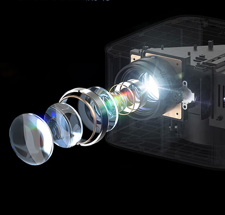
Optical Device Manufacturing
High Purity: Silicon targets ensure the clarity, stability, and accuracy of optical devices, enhancing their performance and reliability. Anti-reflection and protective layers: In fiber optic communications and integrated optical circuits, silicon dioxide films are used as waveguide materials to transmit and process optical signals.
Semiconductor Manufacturing
Used to prepare substrates and packaging materials for LEDs, providng improvement in the luminous efficiency and stability of LEDs.
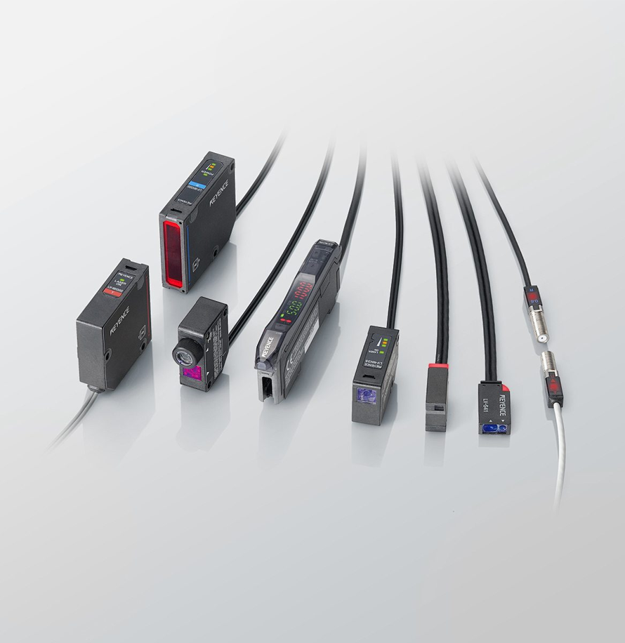
Sensor Manufacturing
Used in the production of sensor elements and signal processing circuits, enhancing the sensitivity and accuracy of sensors
Technical Characteristics

Purity
The purity of crystalline silicon is 99.999%, and the purity of Hsi is 99.99%
Density
2.33 g/cm³
Application Scenarios
Optical Device Manufacturing

Semiconductor Manufacturing
Sensor Manufacturing
Contact Us